


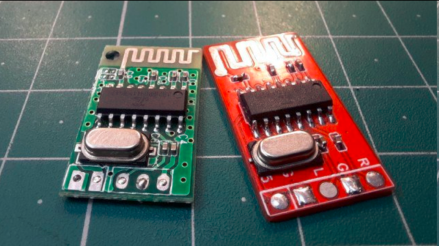
 We have all seen Printed Circuit Board (PCB) antennas: those squiggly bits of traces on PCBs connected often to a Bluetooth, WiFi or other wireless communication chip. On modules like for the ESP8266 and ESP32 platforms the PCB antennas are often integrated onto the module’s PCB, yet even with such a ready-made module it’s possible to completely destroy the effectiveness of this antenna. These and other design issues are discussed in this article by [MisterHW].
It covers a range of examples of poor design, from having ground fill underneath an antenna, to having metal near the antenna, to putting dielectric materials near or on top of the antenna. The effect of all of these issues is generally to attenuate the signal, sometimes to the point where the antenna is essentially useless.


More Stories
via Hackaday: Web-Based Control for a CB Radio
via Hackaday: Does Your Terminal Speak Morse? This One Does
via Hackaday: NASA Announces Artemis III Crew and Ambitious Goals